Electrical Failure Analysis Laboratory (EFA Lab) Introduction

EFA lab is located in T149 room (class 100) of ONPY2 clean rooms. Various tools and techniques are available for FA analysis in EFA Lab. These are Laser cutting, Micro-probing, Semiconductor analyzer, RLC bridge, Liquid crystals, temperature conditioning, Photoemission, and several others as described below. In addition several documents are attached to each tool or technique including application examples in order to help you to decide which technique will be most appropriate for your future FA requests.
Further details can be found in work instructions for EFA Laboratory, located at WWCM under number 12MON24776D.
- The Circuit corporate newsletter
- Article introducing EFA Laboratory in ON Semi News in English
- Article introducing EFA Laboratory in ON Semi News in Slovak
Photoemission Microscope
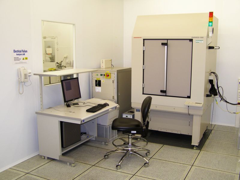

The PHEMOS-1000 Photoemission microscope is built on a low noise, cooled, CCD camera with resolution 1024x1024 pixels. The camera is used to capture the pattern image (optical image of investigated area) as well as photoemission image. These two images are superimposed to create a single image which is the final photoemission image. For connecting of electrical signals to the die (sample) the Karl Suss PM8 double side prober with probe chucks is used. This prober allows front and back side probing directly on wafer. Available chucks in ONPY are: 8" front side chuck and two backside chucks, 6" and 4". The electrical connection can be performed by EG2000 compatible probe cards or by six probe-heads. Two of them (PH150) are designed for micro-probing and the remaining four (PH120) for probing on probe pads. The whole system is controlled by user friendly software from Hamamtsu. Generally, this tool is used for localization of leakages in semiconductors. More details on photoemission system, techniques (Background section), applications and finally practical example of PEM application are shown in the documents below. Work instructions can be found in WWCM under number 12MON24777D.
- Photoemission microscope PHEMOS-1000 in ONPY2
- Introduction of photoemission techniques by Hamamtsu
- PEM application example (missing TiW barrier, PS5LV)
- ON Semi News article
There are further plans to extend this tool with new techniques to grow existing PEM FA opportunities. The important option is Laser scanning, which rapidly increases resolution of the system and most importantly opens the gate to new techniques such as OBIRCH (Optical Beam Induced Resistance Change) and TIVA. These new techniques can be used to localize interlayer leakages and shorts and are important for us (previously observed on issues with broken VIA, voids, etc.). Overview on OBIRCH technique is located in the document below:
Note: PEM is equipped with high resolution solid ink color printer for paper form output from this tool.
DTS tester / Eagle ETS300 tester
This system will be used as alternative to Eagle ETS500 system for conditioning of electrical signals supplied to a sample under photoemission investigation. The tester is electrically interconnected with probe card placed in Photoemission microscope and held by probe card holder (front or backside). A sample is biased with the necessary electrical signals to bring it to failing mode and detect photoemission sites(s). Similar effort can be achieved by application of DC sources which are available in the DC measurement rack described below.
Laser Cutter

Laser cutter was the first tool in ONPY for failure analysis. It includes several parts and covers several techniques from laser cutting through micro-probing, liquid crystals, I-V, impedance characterization, temperature conditioning and measurement automation (GPIB+VEE). The tool was built in ONPY2 from various components. Such configuration is unique over ON Semi corporation. Laser NewWave EzLaze II with two wavelengths near ultra violet (NUV 355 nm) and green (533 nm) can be used for laser cutting. Generally laser cutting is used for electrical isolation of a device in the circuit in order to measure its electrical characteristics without influence of the rest of the circuit. The tool is equipped with A-zoom microscope, which offers adjusting of magnification within specified range without changing an objective. The picture from microscope (during laser cutting) is grabbed by a 3MP CCD camera and there is no direct contact of user with laser radiation. The tool is equipped with front side probe card holder, which can be used for probing of samples by using EG2000 compatible probe cards. Details on this tool can be found in various documents mentioned below.
- Laser cutter in ONPY2 Overview
- Work Instruction, see WWCM documents 12MON23542D and 12MON22866D (written in Slovak)
- Laser Cutter short user's manual
- Laser cutter application example
- Probe card holder
- ON Semi News article
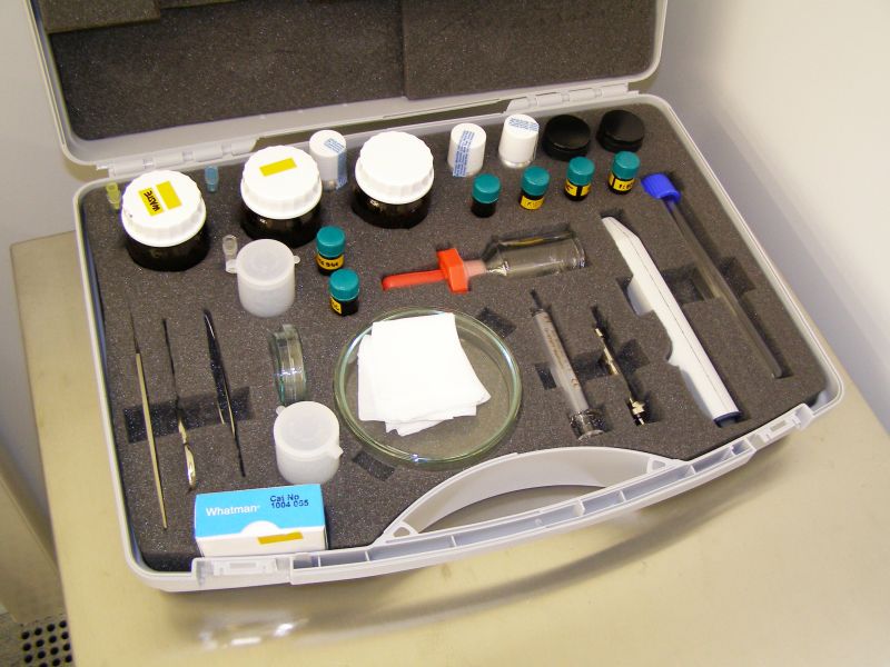
Liquid Crystals
This kit is used for localization of hot spots by help of liquid crystals which have a defined clearance temperature point (when they change their phase. The liquid crystals are applied to sample surface by help of fluid carrier with high evaporation rate (Freon, Sefazone, etc.). In order to see changes in crystal polarization, microscope needs to be equipped with a polarizer and analyzer. The liquid crystals on the surface change its orientation according to the local heat distribution. If there is an area which is overcoming clearance temperature, crystals will get dark at this place (this place is so called hot spot). In most cases this technique is used for localization of areas where is extended heat dissipation and this might be connected directly (metal shorts) or indirectly (overheated power transistors) with the investigated failure. Please note that higher currents through a sample are required in order to detect hot spots by help of Liquid crystals. For instance for K18 liquid crystals with sample temperature 26°C, current around 1 mA is sufficient for detection. Example how a hot spot is detected on a triple metal layer device is captured in the video sequence below (Sample temperature 26°C, current sweep 0.5-2 mA)

Micro-probing

Micro-probing can be performed using the Laser cutter tool. Five precise micro-manipulators (Wentworth SPV200) are available with various needle types. Two types of needles for micro-probing with 0.25 and 0.1 um tip radiuses are available. With such needles it is possible to contact Metal top lines and in some special cases also Metal 2 lines (triple metal, to connect Metal1 lines openings by FIB needs to be done) and perform I-V or Impedance characterization. Note: These needles are sensitive to damage. In case of passivated sample it is appropriate to use laser cutter (NUV) to create openings through the passivation (to Metal top), like micro pads and use them for probing in specific locations (appropriate for metal top). Example of microprobing together with laser cutting performed in EFA Lab can be found in the following document.
C-V, C-t Measurements

C-V, C-t plotter model HP4280A is again part of the Laser cutter system. This tool together with prober and hot chuck are used for measurement of capacitance-voltage and capacitance-time characteristics of MOS structures in order to qualify properties of oxide layers used as gate insulators for all MOS transistors produced in ONPY. The same tests are performed as in-line monitoring in the diffusion area (used short loop material). The advantage of the described tool is high sensitivity (range 2pF), which allows measurement of low capacitance values. Example of measured C-V of NLV transistor (PS5LV) is shown in the figure on the right. Please note capacitance in accumulation region (Cmax) reached value 2.7 pF only.
I-V Characterization

For I-V characterization is used old semiconductor analyzer HP4145B. This instrument is interconnected with PC through GP-IB buss, which is used to store display content to files. The system is similar to newer models (4156) and offers:
4 x SMU (0-100 V, 0-100 mA)
2 x Voltage sources with current compliance
2 x Voltmeter (can be used as differential voltmeter)
Example on IV measurements:
DC Measurement Rack DCR-ONPY-01
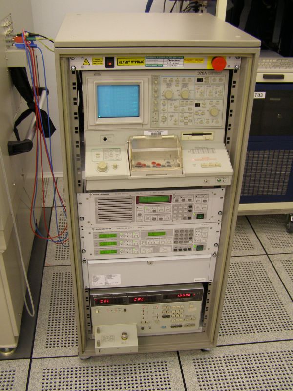
Is used as a mobile set of power sources with curve tracer, signal generator and other future instruments. Due to its mobility, this rack can be used together with Photoemission microscope, Laser cutter or for other purposes as well.
Electrical Specifications:
SONY Tektronix 370A (Programmable curve tracer)
P max: 220 WV max: 2kV
Communication interface: GP-IB
R&S GPX35/10 (DC source):
0-35 V / 0-10A (four-point connection)Communication interface: GP-IB
R&S NGPT35 (DC source):
0-35 V / 0-1A (four-point connection)
0-35 V / 0-1A (four-point connection)
0-7 V / 0-5A (four-point connection)
Communication interface: GP-IB
MOTECH FG503 (3 MHz DDS function generator)
Communication interface: GP-IBHP4191A RF Impedance Analyzer 1-1000MHz
Communication interface: GP-IBRelated documents:
- Work instructions (in Slovak) WWCM 12MON26699D
- Companion technical documentation
- Manuals
Microscope LEICA 1000

Optical microscope for analytical purposes
Available objectives:
- 2.5X standard objective
- 20X, (Leica, dark field, long distance),
- 50X, 80X (Leitz standard objective),
- 150X (Leica, Dark field)
Supported:
- Fluorescent mode,
- Dark Field mode,
- grey filter,
- 5 apertures
Image acquisition:
- 5MegaPixel CMOS industrial Camera (USB2)
- 2D measurement software