Photoemission
Photoemission (PE) also known as photon emission microscopy or just emission microscopy is wide used in failure analysis for detection of failures with very low-level light emissions in integrated circuits. PE occurs when an excess energy generated at a leakage or in a generation-recombination site is radiated out of an electronic device as photons. These photons are detected by sensitive light detectors (e.g. Vidicons, CCD's). PE presents non-destructive passive fault localization technique that involves collecting of photons from failed device, typically biased under normal operating conditions. Superimposing of the photon emission image with reflected light image (so called pattern image) gives the location of a PEM site.
Many defect types in Silicon emit photons with wavelength between 500 and 1300 nm. Usually, photoemission is detected from the front side of an analyzed device. Due to the transparency of silicon in the near IR region it is possible to detect failures from the back side as well.
Photoemission is useful for detection of forward, reverse biased PN junctions, junction leakages, hot electrons, junction avalanche, latch-up, substrate damage, oxide leakages, PolySi filaments, switching FETs in inverters, and several others.
Unfortunately photoemission is not sufficient to detect "Ohmic" leakages, metal interconnect shorts, silicon conduction paths (e.g. diffused resistor), leakage sites under large metal blocks (this can be overcome by back side PE), buried junctions, MOSFETs operated in linear region and few others.
Photoemission mechanism

Light emission from silicon has been observed by Newman in 1955 from reverse-biased PN junction and that from oxides by Solomon and Klein in 1976. Photoemission mechanisms must be explained by quantum mechanical theory and is still not completely understood [4]. In the simplistic model, when energetic carriers recombine in a semiconductor they can lose energy though a photon (lattice vibration) or by emitting a photon of light. The wavelength of these photons is within the range from 850 to 1650 nm, where for Si with band gap 1.12 eV the peak value is 1100 nm as illustrated in Fig. 1. Carriers in indirect band gap semiconductors, such as silicon, preferentially lose energy though photons thus photon emission efficiency is extremely low, estimated to be one photon per 106 to 108 electrons crossing the junction in avalanche breakdown. This leads to the requirement for ultra sensitive light detectors (cryogenically cooled CCDs (charge coupled devices) intensified CCDs, and recently optimized infrared (IR) detectors (InGaAs, HgCdTe, MTC).
Generally, there are three types of photoemission i) from biased p-n junctions and related structures, ii) hot-carrier luminescence and iii) electroluminescence from dielectric films. Recently Akil et. Al. [2] proposed model of luminescence from biased p-n junctions consisting of there different mechanisms operating at different photon energy ranges. i) indirect interband processes (Gautman et al. 1988) for energies below 1.8 to 2 eV, ii) bremsstrahlung radiation (Figielsky and Torun 1962) for mid-energy regions 2 to 2.3 eV, iii) direct interband processes for energies above 2.3 eV. More details on photoemission principle can be found in literature [1, 2]. Summarizing; failure mechanisms that could result in photon emission are:
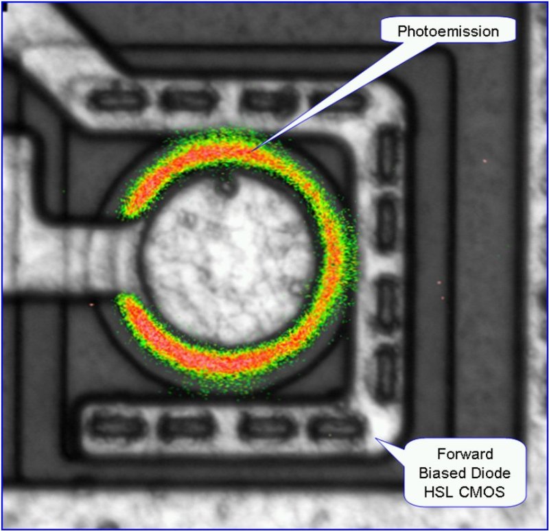
- Recombination of minority carriers in forward biased junctions. In this case minority carriers are injected across the forward biased junction and recombine. Photoemission from forward biased junction is uniform across the junction (Fig. 2). This mechanism is similar to Light Emitting Diode operation except that LED materials are direct band gap materials where photon generation efficiency is much higher due to photons are not required for the transition.
- Reverse biased avalanche breakdown of p-n junctions probably emit though a combination of interband, intraband, and bremsstrahlung methods. Compared to the forward biased junction, it is easier to detect PE. More details can be found in DBL-ISO Zener diode report.
- Contact spiking and PolySi filaments: For failures resulted from contact spiking, where leaky p-n junction is formed by aluminum spiking into n-type region, the photoemission is similar to that of reverse biased p-n junction (Fig. 3). Junction spiking may also result in a localized Silicon Controlled Rectifier (SCR) latch-up event and in extreme situations, when contact spiking results in a short with linear IV characteristic, it may not result in any visible photon emission. Example on ESD leakage caused by Aluminum spiking can be found for example in EFA2007-001 and EFA2008-003 reports.
- Latch-up in CMOS circuits arises when the parasitic NPN and PNP transistors form a regenerative feedback loop causes SCR action [3]. Principal of Latch-up mechanism is illustrated in Fig. 4.
- PolySi filaments can be formed during ESD, EOS stress in CMOS devices. For instance in N-MOSFET, ESD stress can cause the n-type PolySi gate material to melt and migrate through the gate oxide into p-type bulk thus forming a polysilicon filament and poorly formed junction between gate and bulk (substrate). This poorly formed junction under electrical bias generates photon emission similar to the forward or reverse biased junction. Whether or not this photoemission is detectable depends on doping type and doping level difference (bigger difference higher photoemission). If PolySi and substrate are of the same type there is not detectable photoemission. Example can be found in EFA2007-014 report.
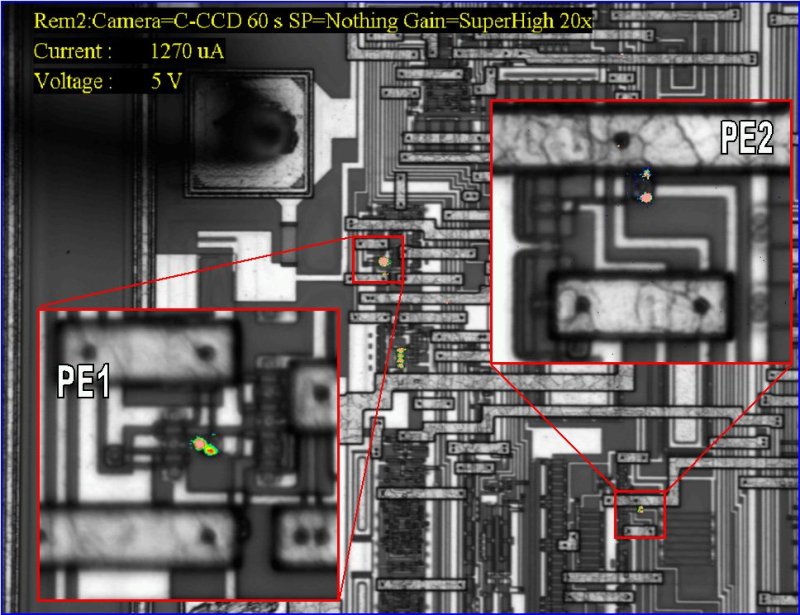
- Saturated MOS transistors. The photoemission is detected at the drain edge as carriers recombine after being accelerated across the pinch-off region and hit the lattice. PE example is shown in Fig. 5, detailed information can be found in [6].
- Oxide breakdown (non-damaged oxide emission) is recombination hot electron tunneling across the oxide (example Fig. 6).
- Oxide damage (pinhole/gate edge ESD damage). Example of pinhole can be found in EFA2007-014 report and one example is shown in Fig. 7.
- Floating gates in CMOS circuits. For more details please refer to following reports: EFA2007-019, EFA2008-001.
Unfortunately, as mentioned above, photoemission is not sufficient to detect "Ohmic" leakages, metal interconnect shorts, silicon conduction paths, leakage sites under large metal blocks (this limitation was overcome by back-side PE), buried junctions, surface inversion leakage caused by mobile ion contamination, PMOS transistor gate leakage (less likely emit), MOS transistors in linear mode [6] and some others.


Photoemission microscope (PEM)
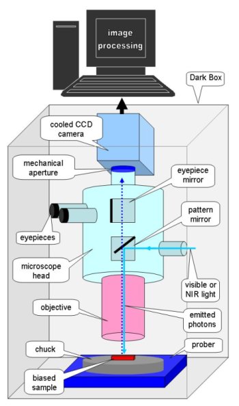
The first photon emission microscope (PEM) was developed in the early 1980s [1]. A typical photoemission microscope (PEM) includes dark box (light tide) containing a conventional topside or/and backside probe station (Karl Suss, Wentworth, Cascade etc.), an optical microscope (Mitutoyo, Nikon, etc.) and cooled CCD camera (Hamamtsu, Quantum Focus, Hypervision). Principal schematic of PEM is shown in Fig. 8. Usually, low current measurements may not be required, but a hot chuck as an option might be helpful because some samples are failing at specific temperature and emission may depend on it. PEM practically works in two modes; i) pattern (reflected light image) and ii) photoemission.
In the pattern mode, illustrated in Fig. 8, the PEM is used as regular optical microscope to grab an optical image of a sample pattern. In the case of front side investigation, the light (within the visible range) is passing through half mirror, optics (available objectives with magnification usually 5x, 20x, 100x) and reaches the sample surface. The light from sample surface is reflected back and passes the same way, crossing half mirror and continuing straightforward to the CCD detector respectively to eyepieces. Please note eyepieces can be used only for front side investigation.
In the photoemission mode, illustrated in Fig. 9, photons from a biased sample are passing through optics (available objectives with magnification usually 5x, 20x, 100x and macro objective <1x) directly to the NIR detector (CCD camera). Optics is optimized by coating for near IR (NIR) region covering visible spectrum as well. In order to decrease noise level of the detector, the CCD camera is cooled to temperatures around -50°C (realized by Peltier elements) and even less for MTC (HgCdTe), InGaAs (liquid nitrogen, LN2). Even with cooling the noise level is significant. Therefore after first photoemission the second one is required but with unbiased sample. This image is called dark image and is extracted from first PE image. Both images (PE and pattern) are stored in computer buffer and at the end superimposed to the final photoemission image, where PE center is localized within the sample reflected pattern.

IR Detectors for PEM
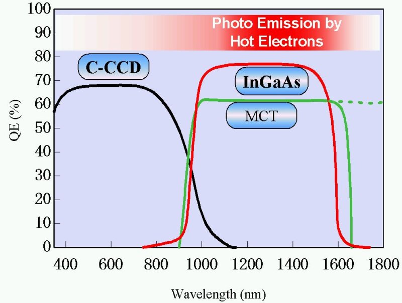
There are several types of IR detectors. Currently the most common type is cooled CCD (Charge Coupled Device). As was already mentioned cooling is used in order to decrease noise level of a used detector. Temperature is usually in range about -50 to -70°C, for Si CCD (cooled by Peltier elements and chiller), and lower for MTC (HgCdTe), InGaAs detectors (cooled by liquid nitrogen). This cooling is important for long exposition times where low readout rates are employed (typical readout noise of CCD operating at room temperature is about 30 electrons (RMS) at readout frequency 1 MHz) [1]. Even at such low temperatures the CCD noise is not negligible and therefore after first counting of photons from biased sample the counting is repeated for the unbiased sample. Thus the dark image (dark noise) is obtained and further excluded from grabbed photoemission images. Offered detectors have different spectral and efficiency properties as summarized in Fig. 10 (Hamamtsu 2007). Practical sensitivity comparison of individual detectors, provided by Hamamtsu (2007) is shown in Fig. 11.

Front-Side photoemission
Photons are counted and pattern image is obtained from a top side (active side) of the sample. In this mode the light within visible range is used to acquire pattern image. The front side photoemission is easy applicable and is appropriate for samples with less than two metal layers. If the photoemission is generated under the metal the photoemission cannot be observed. For some cases if the macro objective is used it is possible to see even such photoemissions. If such situation is observed it is the right time to switch to back side photoemission. Few examples on front-side PE can be for example found in following EFA reports:
- EFA2007-012 NCP1583 (incomplete contact etch)
- EFA2007-019 NCP3418 (incomplete contact etch)
- EFA2008-02 oxide breakdown caused by plasma damage
Back-Side photoemission

Due to the optical properties of Silicon (Eg=1.12eV), it is transparent for light with wavelengths near infrared region (1100 nm). Therefore it is possible to see pattern image and detect photons generated from the sample back side. Usually, in this mode the pattern image is obtained by help of IR light, which is passing through the substrate (Si), reflects from top side of the sample (e.g. from metals, PolySi) and returns back.
The amount of reflections and thus pattern image quality strictly depends on thickness of the substrate material. It is recommended to use as sample thinned as much as possible. Practically speaking the recommended thickness is 50-100 um. For thicker samples the pattern image quality rapidly decreases with thickness of the sample. Example of hardware configuration during backside PE is shown in Fig. 13. The quality of the pattern image can be marginally improved by application of laser scanning (confocal microscope). In this case even thicker samples can be used for investigation. Several examples of application of backside PE are listed in few EFE reports below:
- IR backlight pattern vs. laser scanning pattern
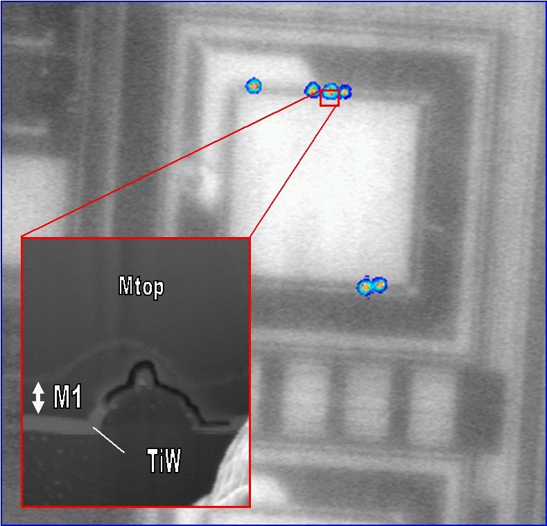
- EFA2007-001 (missing TiW barrier)
- EFA2008-003 (missing TiW barrier)
Further techniques, upgrading EFA PEM hardware
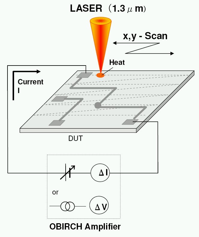
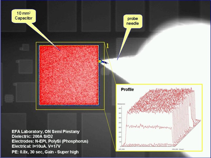
There are several supported techniques which can be added to existing ONPY Phemos-1000 tool. The backside pattern image can be essentially improved by using laser scanning. In addition the laser scanning is involved in other important analytical technique called OBIRCH (Optical Beam Induced Resistor Change). This technique is sensitive to problems that cannot be detected by photoemission, like "Ohmic" leakages and metal interconnect shorts. The laser is scanned across the sample to locally heat the area , consequently the current (resp. voltage) is recorded respective to laser beam position. If there is a place sensitive to temperature it will result in a current or voltage change. The result of OBIRCH (Hamamtsu) analysis is a patterned image with colored locations where the resistivity was changed by laser stimulation. Generally two colors are presented one for resistance increase and another for resistance drop. This analytical technique is offered by several producers [8, 9] and has several names like TIVA, XIVA, etc. Similar to OBIRCH effort can be obtained by another analytical technique called thermo emission. The principle is similar to the photoemission just, detected is Joule heat within spectral response in the range 3-5 um. The photoemission microscope can be equipped with laser marker, which is useful for marking of PEM locations for example within large capacitors. More details regarding OBIRCH, TIVA, and thermo-emission can be found in [1, 7]. See related documents for details:
Literature
[1] "Semiconductor Device and Failure Analysis, Using Photon Emission Microscopy", Wai Kin Chim, Wiley, 2000, ISBN047149240X[2] "A multimechanism model for photon generation by silicon junctions in avalanche breakdown", Akil, N., Kerns, S. E., Kerns, D. V. , Hoffmann, A. And Charles, J. P., IEEE Trans. Electron Devices, 46 (5), 1022, 1999
[3] "Electroluminiscence measurements with temporal and spatial resolution for CMOS latch-up investigations", Qionckle, J., Boit, C. and Fuhrer, D., Microelectronic Engineering, 12, 157, 1990
[4] "Photoemission Microscopy Overview", Jim Mohr, Product Analysis Lab
[5] "Photo Emission and Laser Scanning Methods with the Phemos 1000 System", Thomas Niiederreiichhollz, 2006
[6] "Photoemission of the NLV MOSFET (SK)", M. Ziga, 2007
[7] "Failure Analysis for Yield Enhancement", David L. Burgess, 2007
[8] Quantum Focus web pages, http://www.quantumfocus.com/
[9] Hypervision Inc.