Concluding words
It is time to provide final statement on EFA activity. Briefly from history, EFA Laboratory was established by Valentin Kulikov in 2007 in an area of the ONPY2 clean room which was previously used for storing scrap wafers. It must be noted that such laboratory is important part of each semiconductor FAB, helping to solve problems in the production line to enhance process and probe yields. In addition to the primary mission of the laboratory to support failure analysis for internal customers, the EFA Laboratory also participated on numerous failure analyses for other external ON Semi sites including: BDC, RDC and others. Three internship students were working in the laboratory during its existence. Their work was great addition to the laboratory success and is published on these WEB pages in section others. Up to now EFA laboratory reported more than 50 FA reports, describing individual issues and recommended solutions. All of them can be found at following link \\Bezovec\efa\Reports in PDF format. Please note that during whole EFA Lab existence there was only a single engineer working on FAs (decision driven by management). At the end I would like thank to all colleagues, who helped to build EFA Lab and helped to its expansion and development. It was shown that it was possible to build analytical laboratory in Piestany with corporate quality level. Thank you all again... Valentin Kulikov, Piestany June 2009General Introduction

Failure Analysis (FA) is the process of determining how and why a semiconductor device has failed. FA is performed as a series of steps known as FA techniques. In other words FA searches for a root cause of failure with the goal to identify a failure mode, a failure site and a failure mechanism. The results from failure analysis allow us to improve product reliability and yields Electrical failure can either be functional or parametric. Functional failure refers to the inability of a device to perform its intended function. Parametric failure refers to the inability of a device to meet electrical specifications for measurable characteristics (such as leakage current) that does not directly relate to functionality. Thus, a parametric failure may be present even if the device is still functional or able to perform its intended function. For example, a DAC (Digital to analog converter) that can convert digital data into the correct analog voltage but draws excessive supply current is a parametric failure, but one that does not convert data at all is a functional failure.
Failure analysis process
In order to optimally distribute FA resources it is important to first validate the reported failure prior to failure analysis. Failure verification is also done to characterize the failure mode. Good characterization of the failure mode is necessary to make the FA process efficient and accurate. Failure verification is followed by performing various FA techniques step by step on a sample to collect attributes and other observations along the way. Non-destructive FA techniques are done before destructive ones. Also results of these various FA techniques must be consistent or corroborative. Any inconsistency in results must be resolved before proceeding to the next step. For example, a pin that exhibits a broken wire during X-ray inspection but also shows an acceptable curve trace during curve tracing can not happen, so this inconsistency must be resolved by verifying which of the two results is correct. In general, the results of the various FA techniques would collectively point to the real failure site. The FA process is finished once there is enough information to make a conclusion about the location of the failure site and cause or mechanism of failure.
About FA opportunities in ONPY2 Piestany
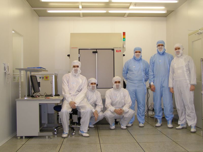
Electrical Failure Analysis Laboratory (EFA Lab) was built in 2007 in an area of the ONPY2 clean rooms. The main goal was to create a laboratory which will support FA activities directly on site in order to minimize investigation cycle time. The laboratory is located in the T149 room, which was created from wafer storage room and part of epitaxi room obtaining class 100. Primary focus of the EFA Lab is to support ONPY manufacturing facilities where the main goal is to prevent line down situations caused by accidental process issues, equipment failures, and other. The secondary activity of EFA Lab is support of other tasks such are yield improvements, new product development (during corrective action cycle) and other for internal as well as for external customers. Please note, activities on external customer returns are covered by ON Semiconductor Product Analysis Laboratories (PAL) in PHX, OSPI, Seremban, Roznov. The highest priority of EFA lab is support of ONPY production line.
How to request FA/Support from EFA Lab?

Please see section “Analysis request” for most recent information.
Future Plans:
EFA Lab would like to be to be a part of the PAL group, sharing corporate Product Analysis Management System (PAMS) where you will be able easily create a FA request by submitting the electronic form
Who is the right contact person for you to answer your questions?
 Responsible for the laboratory is Valentin Kulikov, who with help of other people from various departments (Equipment, Facility and others) built this lab. Please see Acknowledge page on the left for a list of people involved with this project.
Several device engineers were trained to work with tools in the Lab and they are:
Trained Photoemission Microscope operators:
Mojmir PripkoJuraj Bobula
Juraj Solar
Trained Laser Cutter operators:
Mojmir PripkoI-V measurement:
All device engineers (Agilen 4155, situated at Probe area)Equipment engineers:
Miroslav StefanovicJozef Kovacik Jr.