Personal Data
 Name: Valentin Kulikov
Date of birth: 25.05.1974
Nationality: Slovak
Status: Married, 1 child
Address: Hlboka 6, 97251 Handlova, Slovak Republic
Phone: +421 908 170 480
e-mail: valentin.kulikov@vvku.eu
Keywords: Microelectronics, Design,
Layout, Failure Analysis, Semiconductor,
high level, expert, result driven
Academic Education
1994 – 1997
Slovak University of Technology in Bratislava. In 1996 obtained academic degree: "Bachelor" in Electronic (Faculty of Electrical Engineering and Information Technology)
 1997 – 1998
Forschungzentrum Jülich, Institut für Ionen- und Schicht-technik, Diploma work with subject: „Design and realization of computer controlled measurement systems for the evaluation of direct-current (DC) and high-frequency (HF) parameters of novel electronic devices“.
in June 1999
Slovak University of Technology in Bratislava
Obtained academic degree: Engineer, Ing. (specialization Microelectronics)
Diploma (SK), Diploma (DE), Defense ratings (DE), University Ratings (DE)
Open diploma work (rated as the best elaborated work).
 from 1999
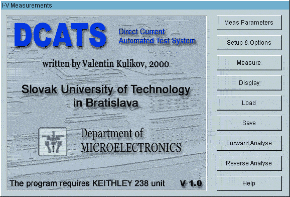
Slovak University of Technology in Bratislava, beginning of the Ph.D. work under supervising by Prof. D. Donoval (department of Microelectronics). This work resulted in developed set-up for measurement and basic characterization of Schottky diodes DCATS [8, 9]. Study was temporary interrupted in 2000 (due to the research opportunity in sensor Group at University in Regensburg, supervising Prof. V. M. Mirsky).
 2000-2004
University Regensburg (Institute of Analytical Chemistry, Chemo- and Biosensors, Prof. Wolfbeis). Obtained stipendium for research work on evaluation of completely automated combinatorial electropolymerization concept and its application for gas sensors (supported by BMBF Project, Kombisens) [1-5, 11-16]. Simultaneously, Ph.D. thesis at Technical University in Munich under supervising by Prof. Dr.-Ing. A. W. Koch.
![]() February 2004
February 2004
Obtained DFG fellowship (three months), subject: Adaptation of the developed electro polymerization concept for evaluation of biosensors
![]() November 2004
November 2004
Obtained academic degree: Dr.-Ing. (under supervising by Prof. Dr.-Ing. A. W. Koch, defended at Technical University Munich, Germany, Department of Electrical Engineering and Information Technology, Lehrstuhl für Messsystem- und Sensortechnik)
Subject: "Equipment for combinatorial electropolymerization
and high-throughput screening of electrical properties
of the synthesized polymers", Supervisor: Prof. A. W. Koch, TUM Munich (MST), [10]
![]() December 2005
December 2005
Obtained academic degree: PhD. (defended at Slovak university of technology), Supervisor: Prof. D. Donoval, FEI-STU
Languages
- German (read and spoken)
- English (read, written and spoken)
- Russian (read, written and spoken)
- Czech (read and spoken)
- Slovak (mother tongues)
Work experience
![]() 1997 – 1998
1997 – 1998
Evaluation of the DC, high frequency, optical measurements and basic analysis for HEMT transistors and MSM detectors (Forschungzentrum Jülich, Germany, Student work contract) [8].
 2000 - 2004
University Regensburg (Institute of Analytical Chemistry, Chemo- and Biosensors, Prof. Wolfbeis), research work contract
- Evaluation of the complete system for combinatorial electrochemical synthesis of polymers on direct electrode arrays (involving 96) special interdigital electrodes
- layout design of the microelectrode array (see patent for more information)
- Design and realization of the measurement concept, comprehensive measurement advance and set-up for high-throughput screening of synthesized polymers in application for detection of gaseous hydrogen chloride (for fire alarms, cable isolation burning). Measurements involved simultaneous two- and four-point DC measurement technique. Note: the first application for polymeric systems.
- The set-up design was provided on hardware and software level.
- Adaptation of the developed system for evaluation of biosensors and planned for semiconductor circuits.
More information can be found in [10]
![]() October 2003 - June 2004
October 2003 - June 2004
PreSens - Precision Sensing GmbH, (artwork, digital photography, photo-documentation of company products, web-design)
 June 2004 - June 2009
ON Semiconductor (formerly MOTOROLA), Slovakia, hired as Device Engineer (Semiconductor production) www.onsemi.com
- September 2004: Project Leader for PowerSense 3 technology transfer (BCD technology transfer from EG USA to Piestany FAB). Transfer successfully completed. Following in active work on Yield enhancement projects as start to be selected for leading new failure analysis field in Piestany.
- May 2005: ON Semiconductor Slovakia, Failure Analytical manager / engineer supervising university students and FA Piestany team members. Purchase whale FA lab equipment, installing, trainings, lab management, etc. Internal and external customer support, attending at audits, quality meetings, and others. Cooperation with corporate FA laboratories.
- 2006: member of high level Process Integration Group
- 2005-2009: Cooperation with Slovak Technical University (projects, opponent reviews for Diploma and Ph.D. Works, etc.)
- Aug.-Sept.2006: Direct supervising of two internship students (from Slovak Technical University. Project topic: “HW design of Hall effect joystick and thermo jogger controller for Laser cutter. Electrical Analysis of integrated circuits, produced by PowerSense technology”. Go to details...
- Aug.-Sept. 2007: Direct supervising of internship student (from Technical University in Kosice). Subject: “Diagnostics and defects detection for semiconductor devices using photon emission microscopy”. Go to details...
- June 2009: Built Failure Analysis Laboratory, LAB management, obtained Lean Six Sigma Greenbelt certificate,
- June 2009: FAB Closure, working for ON semiconductor for 5 years in field of project leading, failure analyses, FA laboratory establishing and management
 From July 2009
Work on different private projects, based on LED technology and others

March 2010 - October 2010
OMS Slovakia, Luminaire producer
Position: R&D Manager, LED Department
- Member of Zhaga standardization worldwide consortium
- Active participation on Light and Building exhibition in Frankfurt
- Participation on various Workshops in Lighting topics
From November 2010
ON Semiconductor Piestany, Slovakia, www.onsemi.com
Senior Application Engineer for Solution Engineering Center,
- Setting up SEC work bench, engineering and administrative tasks including work instructions, ESD rules and other related items.
- NCT75 temperature sensor application note released
- Blue Eye for ON semiconductor, Webcast supported
- CAT4101 thermal foldback application note and Calculator
- CAT4101 thermal foldback Webcast
- Solar Lamp application note (coauthoring)
- Solar-Powered LED Lamp for Energy Savings, webcast
- Work on dynamic load control circuitry
Certificates & Trainings
- Lean Six Sigma Green Belt (ON Semiconductor, 2009)
- Electronic Failure Device Analysis Society - EDFAS Member (ID #538098 since 9/25/2007)
- §25 MPSVaR SR č. 718 / 2002 Z.z. §23 - Elektrotechnik na riadenie cinnosti alebo prevadzky (2009)
- Failure Analysis for Yield Enhancement, Glasgow, Scotland 2008
- Team building and assertivity
- Effective communication basics, Piestany 2007
- Motivation rules
- How to talk to difficult customer
Expertise
- Team building and management
- Problem solving, planning, result orientation
- FA couching and support (FA-Failure Analysis, also applicable for other areas)
- Reporting, internal / external communication
- Coordination of priorities and LAB activity tracking
- Enforcing laboratory results, internal seminars etc.
- Strong communication skills
- Experience with dual FIB, SEM (foc. Ion Beam, FEI-825)
- Experienced in photoemission microscopy, liquid crystals, probing, micro-probing, laser cutting, de-processing, de-capsulation, de-lineation, layout tracking, report writing, lab management and many others.
- Semiconductor FAB processing (from raw material entry till assembly including process, procedures, probing, etc.)
- Process optimization (obtained by Lean six sigma green belt certificate)
- Electronic, mechanic prototyping and design
- Microelectronics layout design (experiences with electrodes, electrode arrays for sensors, ICs, etc.)
- Process and Measurement automatization (GPIB, Serial, TCP/IP, USB…)
Other skills
Software:
MS Office (Power Point, Excel with Visual Basic, Word), MS-DOS, MS Windows 95, 98ME, NT4.0WS, 2000, XP, Adobe Acrobat, Adobe Photoshop, Corel Draw, AutoCad 2000 (2D, 3D), Protel, Altium, Eagle, PADS (Schematics, PCB designs), Microcalc Origin, JMP Statistical, Mentor, Cadence (IC Layout), others
Hardware:
- electronic circuits (Analog, Digital, Mixed), PCB layout design (Protel 99, Eagle)
- Application of micro-controllers (practical experience with MCU ATMEL, Microchip, ISP, Debug Wire (PIC12CX, PIC16CX, Attiny, ATMega, AT90S4X), HD 44780 etc.)
- Mechanical design (Corel Draw 7.0-12, Autocad 200X)
- Semiconductor technology, Layout, Mask, etc. for electronics devices and sensors (Autocad 200X, GDSII conversions)
- Practical experiences with GP-IB, TCP-IP, Serial, Parallel.
- DC, AC, high frequency (practical experiences with instruments such as. Keithley: 617, 238, 2400, 2000, KPC 488.2, HP 4155, Agilent 4156, Tektronix TDS1012, TDS3014, FEI 825, and many others).
Programming languages:
- Microchip and AVR Assembler, C
- C++, Visual C++, Visual Basic
- HP VEE 5-9 (for measurement control and automatization)
- Lab View (for measurement control and automatization)
- ForeHelp (MS Windows HELP writing), html programming, basic experiences with Java
Hobbies
Literature (Science Fiction, Fantasy, Stephen King, Michael Crichton, ...), Traveling (architecture, life and people in foreign countries), Film (Science Fiction, Disney), Bicycle (to overcome short distances), In-line scatting (fun with friends), Tennis, Chess, Theater (real Atmosphere), 3D-Cinema (new experience), Model completing (model airplanes, model boats, model cars, etc.), Electronics-Design (interesting circuits for making life easier), Photography (to catch the best moments of life), RC flight, cars, boats.