Failure Analysis Background, ON Semiconductor
 Established and managed Electrical Failure analysis Laboratory for ON semiconductor Piestany (including budget, tool selection, purchasing, trainings, documentation, work instructions etc.).
More details in PDF document (300kB)
See clone of EFA Web pages for result details...
Absolved trainings and expertise:
- Dual Focused Ion Beam FEI825i (by vendor)
- Sela MC 600 sub-micron cleaving tool (by vendor)
- Photoemission Phemos-1000 Frontside / backside / OBIRCH (by vendor)
- Laser Cutter (Product Analysis Lab, ON corporate, Phoenix)
- Liquid crystals for hot spot detection (Product Analysis Lab, ON corporate, Phoenix)
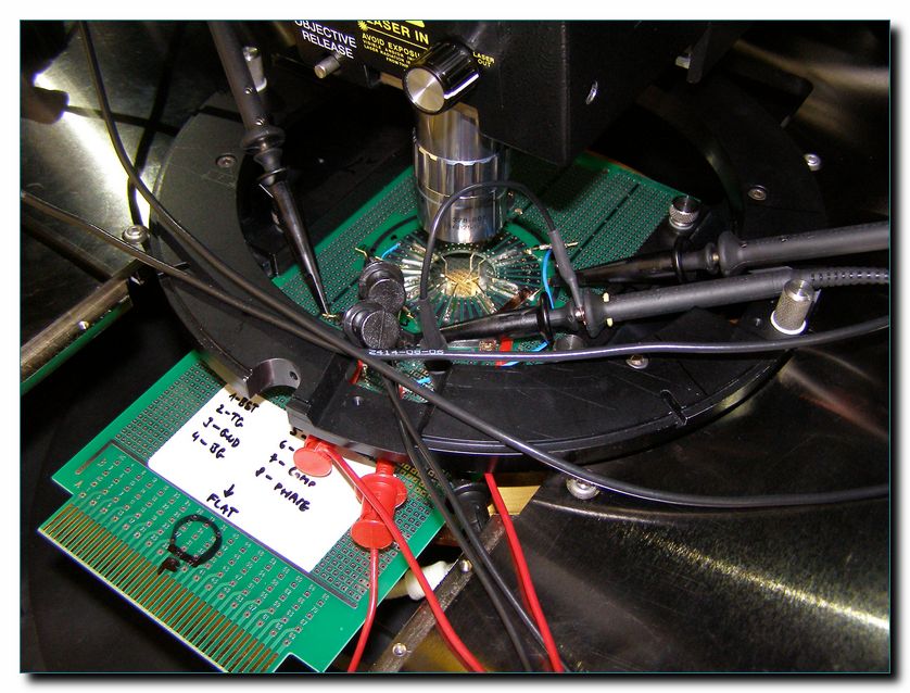
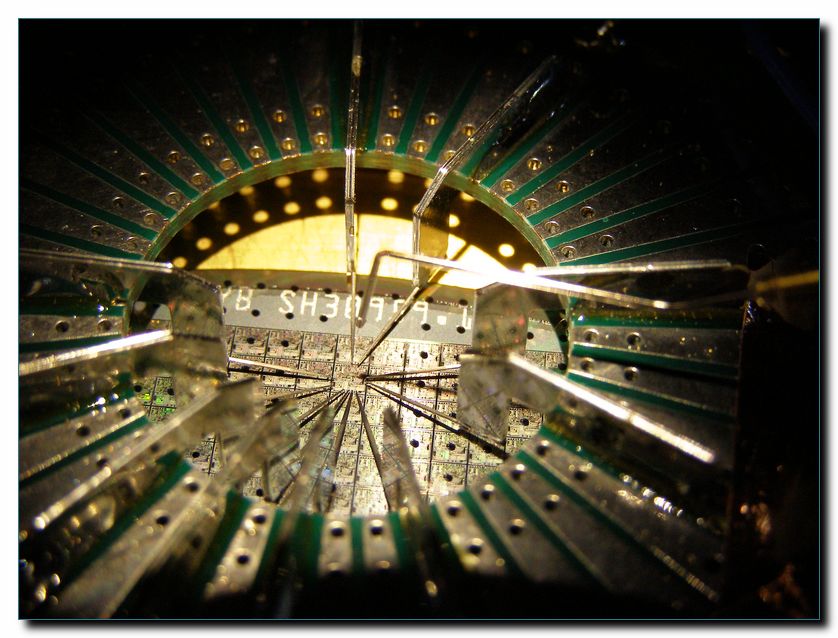
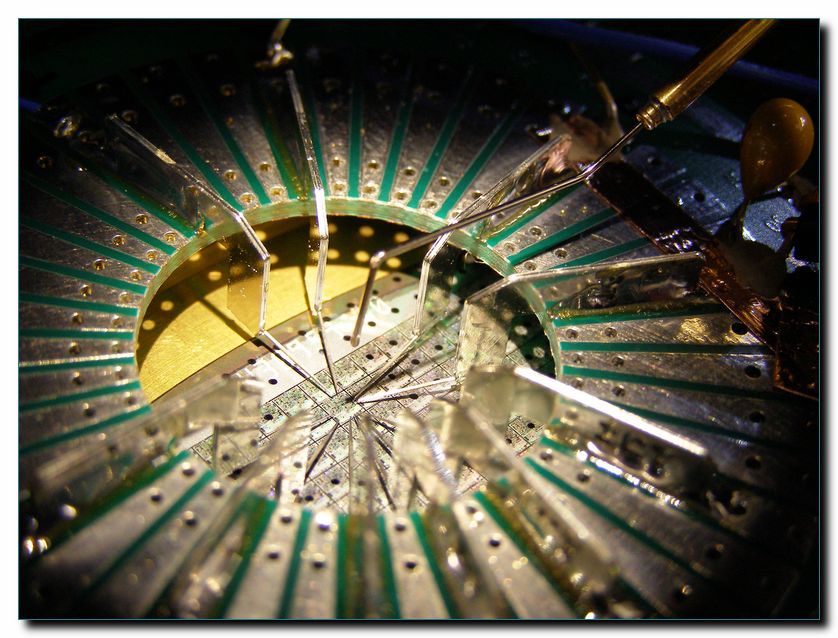
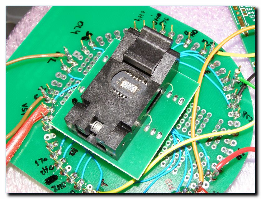
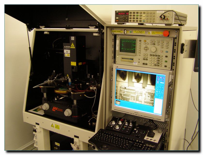
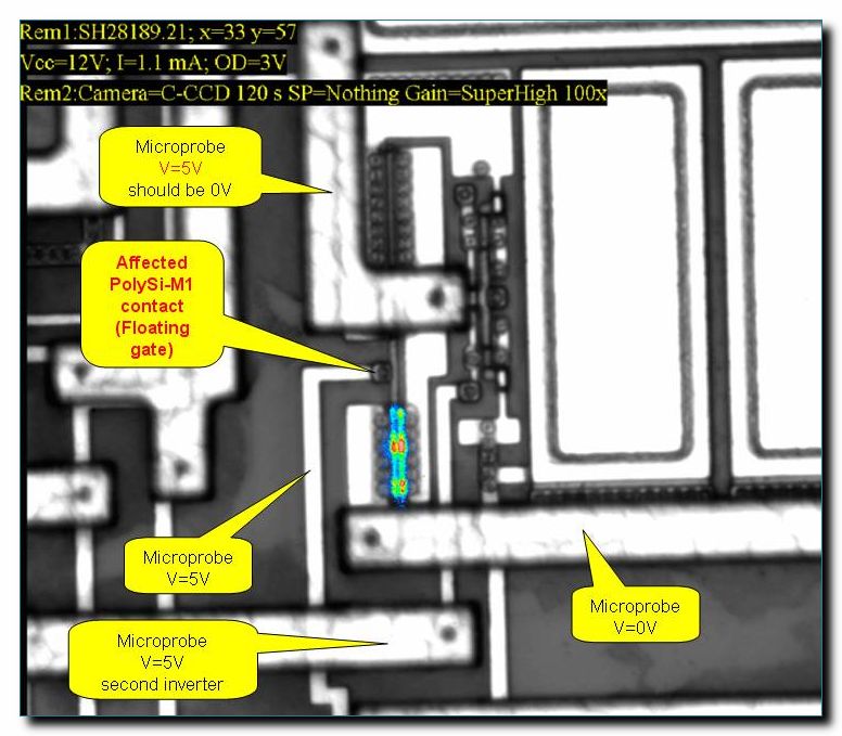
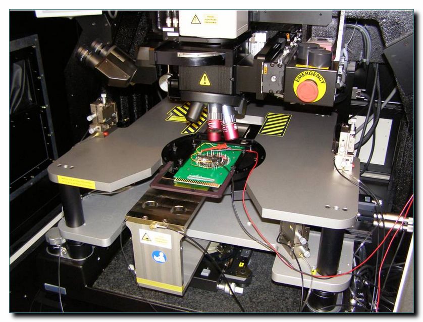
- Microprobe (Product Analysis Lab, ON corporate)
- IV characterization, Impedance measurements
- Decapsulation of ICs (1,6MB)
- Deprocessing to required layer
- Layer Delineation
- others...
Awards
Laser cutter, component selection, purchasing, completing...
For excellent FA coverage providing...
Attended Seminars
- Failure Analysis for Yield Enhancement by David L Burgess, provided by Accelerated Analysis, Glasgow, Scotland, 3-7 September 2007
- Electronic Failure Device Analysis Society - EDFAS Member (ID #538098 since 9/25/2007)
Several written works
Open photoemission report (890 kB)
Open OBIRCH report (1.7 MB)
Open Laser cutter report (735 kB)
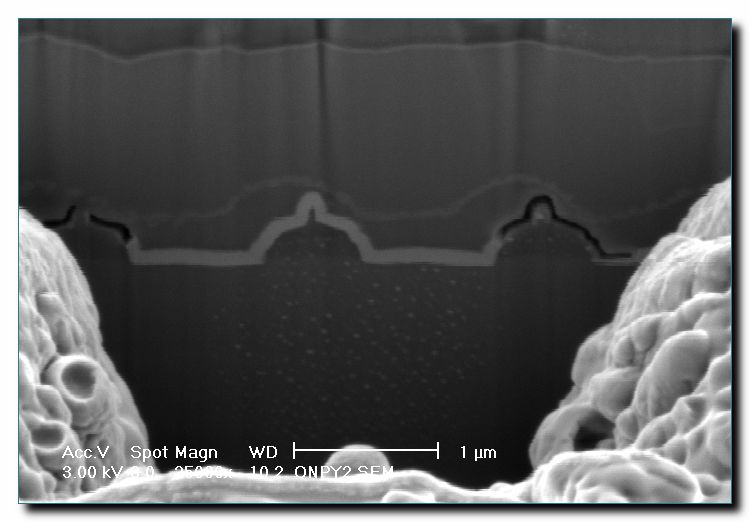
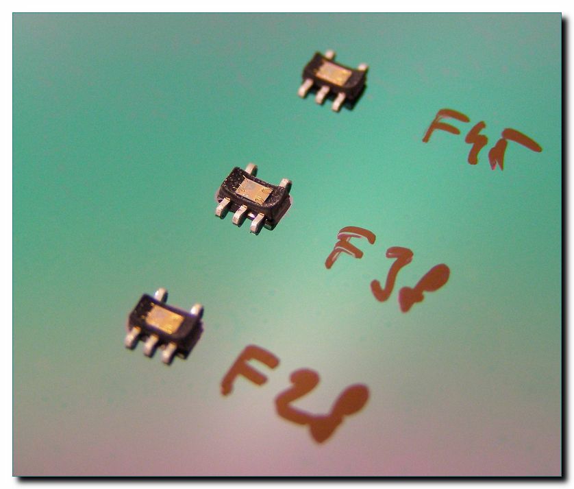
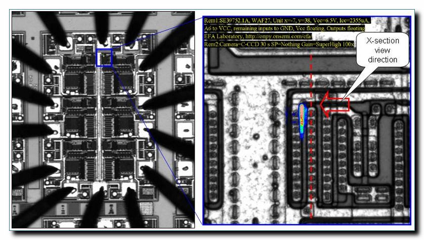
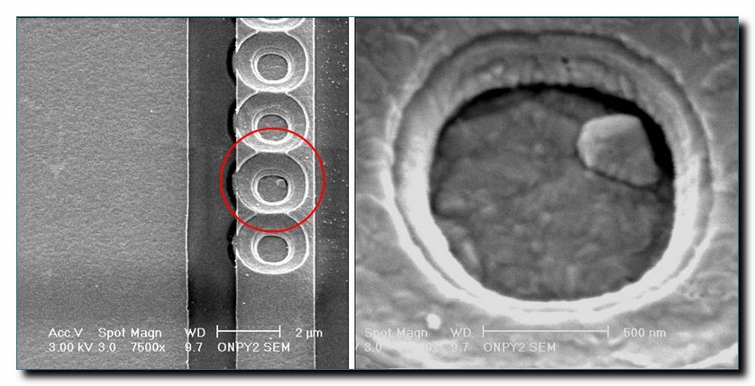
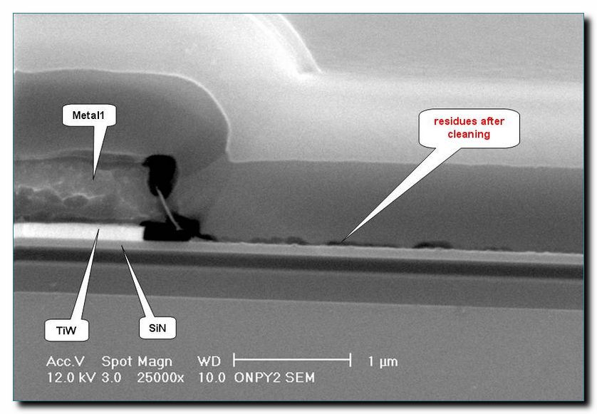
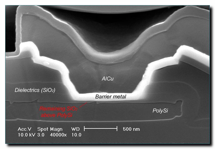
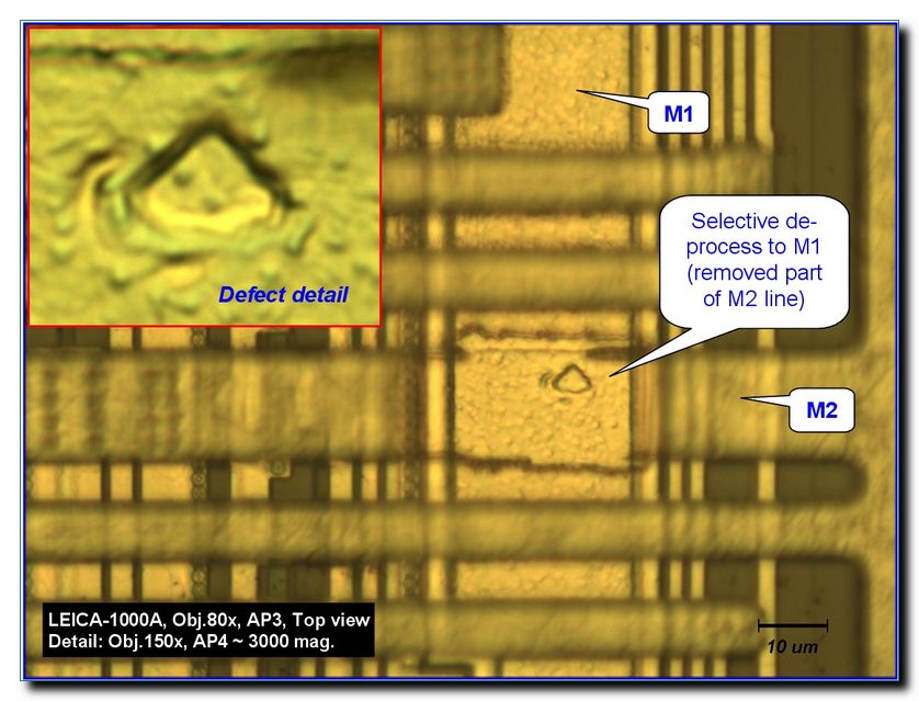
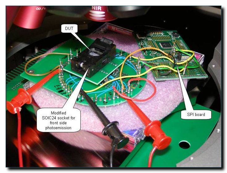
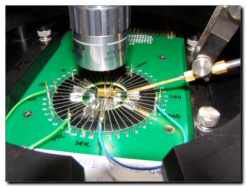
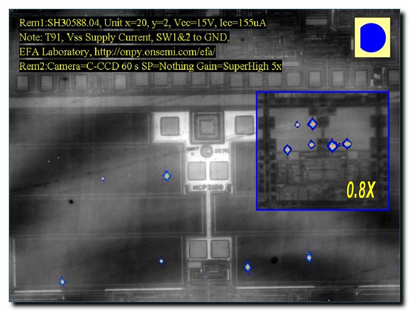
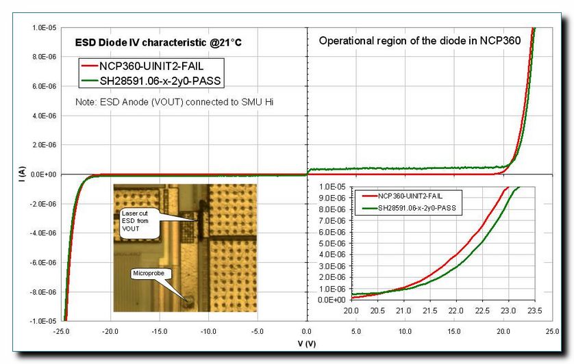
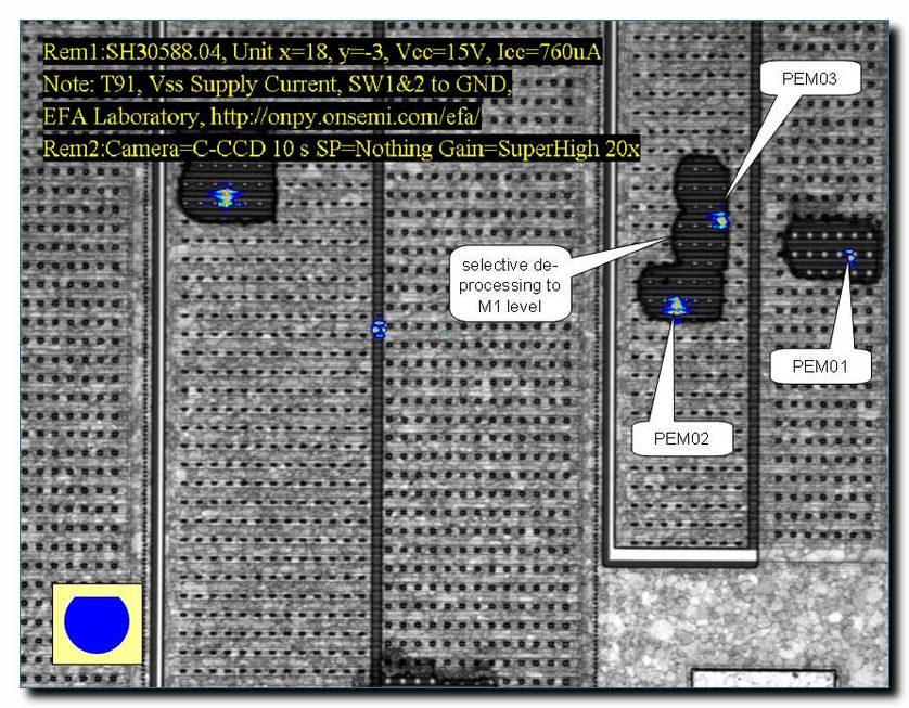
Images from numerous FA reports (reports are proprietary of ON Semi)
 |
 |
 |
 |
 |
 |
 |
 |
 |
 |
 |
 |
 |
 |
 |
 |
 |
 |
 |
 |
 |
 |
 |
 |
 |
 |
 |
 |
 |
 |